Facilities
TMI fosters a campus-wide network that brings together multiple research and tenure-track faculty members, staff scientists, postdoctoral fellows, and students with diverse interests.
Experimental Facilities
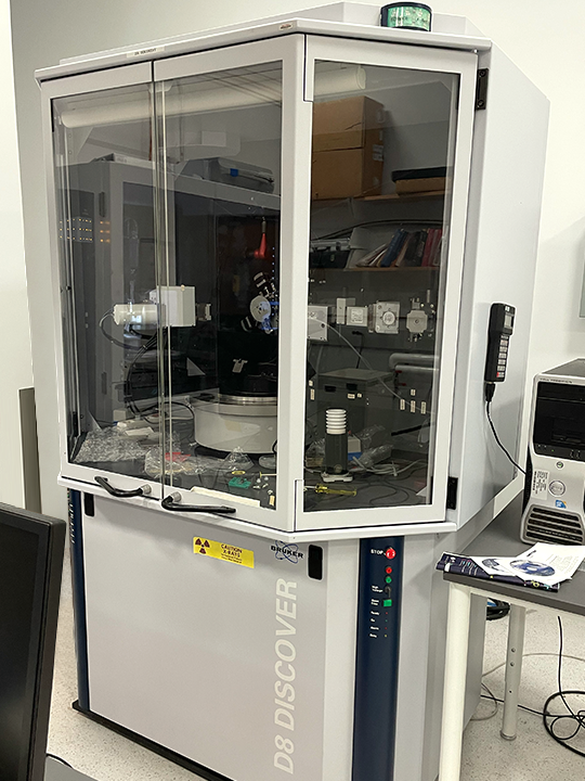

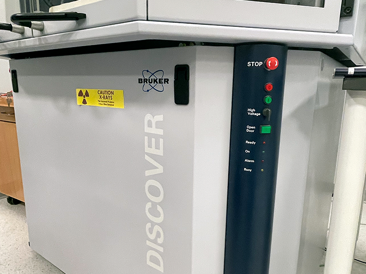
Bruker D8 Discover X-ray Diffractometer
Contact Person: Ke Chen
Department: Physics Dept.
Location: SERC 010
This is optimized for determination of thin film structures. Common applications include high-resolution X-ray diffraction (symmetric/asymmetric peak scans, rocking curves), grazing-incidence XRD (GIXRD), X-Ray Reflectivity (XRR), reciprocal space maps, texture (pole figure) and residual stress analysis. The D8 Discover diffractometer can also be reconfigured for powder diffraction applications. Bruker’s EVA and LEPTOS programs are installed in the system PC for data analysis and simulation.
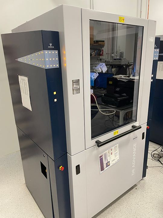

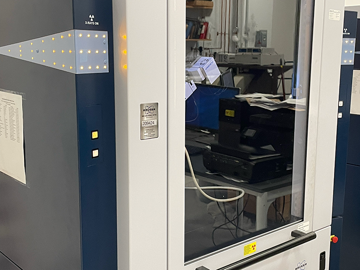
Bruker D8 Advance X-ray Powder Diffractometer
Contact Person: Steven M Chemtob
Department: Environmental Dept.
Location: SERC 010
Bruker D8 Advance X-ray Powder Diffractometer 2kW Cu powder diffractometer with a 9-sample exchange stage, equipped with DAVINCI module including intelligent beam path components providing true plug-and-play functionality requiring minimum or even no user intervention, featuring automatic and tool-free switching of the diffraction geometry without the need for complex adjustments. It is suitable for quick measurement on multiple bulk and powder samples.


JEOL JEM-3010 Transmission Electron Microscope
Contact Person: Ke Chen
Department: Physics Dept.
Location: SERC 008
JEOL JEM-3010 Transmission Electron Microscope 300 kV TEM with LaB6 filament. The acceleration voltage can be adjusted from 100 to 300 kV. The resolution is up to 0.14 nm in lattice image and 0.17 nm in point image. The image can be recorded by a Gatan Orius CCD camera with 4K resolution. Sample loading rod has a single axis rotating up to ±40°. TEM, EDS, STEM, and CBED can be carried out. It is a useful tool for nanomaterial analysis.
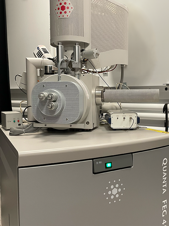


FEI Quanta 450FEG Scanning Electron Microscope
Contact Person: Dmitriy A. Dikin
Department: Engineering Dept.
Location: SERC 008
Capability to work at low vacuum mode to analyze biological samples. The acceleration voltage can be adjusted from 1 to 30 kV. The resolution is up to 1.0 nm at high vacuum and 1.4 nm at low vacuum. It is equipped with second and backscattered electron detectors and EDS. It is also equipped with a fast blanking apparatus to facilitate electron beam lithography operated by the integrated FEI software. This nanotechnology tool addresses the need to investigate a wide variety of materials and characterize structure and composition.


D8 Venture
Contact Person: Michael J. Zdilla
Department: Chemistry Dept.
Location: SERC 010
The D8 VENTURE provides a more spacious enclosure for your experiment with more room for rotating anode, liquid metal jet and dual wavelengths solutions. All systems feature the revolutionary PHOTON III photon-counting detector. The D8 VENTURE offers highest experimental flexibility, with excellent sample accessibility and visibility. It is engineered with high modularity from best-in-class components and is available in popular all-air-cooled configurations. Easy upgradeability protects your investment with maximum flexibility for future extensions.


Bruker Apex II Duo X-ray Diffractometer
Contact Person: Michael J. Zdilla
Department: Chemistry Dept.
Location: SERC 010
Designed for structural determination of single crystals of small molecules (typically less than 500 non-hydrogen atoms). The diffractometer combines a molybdenum X-ray source for high throughput and charge density experiments, and a copper source for absolute configuration and protein screening. The APEX2 software has a graphical user interface that guides the user through the complete experiment and analysis, from data acquisition through data collection, integration and scaling to structure solution and refinement and report generation.


JEOL JEM-1400 Transmission Electron Microscope
Contact Person: Daniel R. Strongin
Department: Chemistry Dept.
Location: SERC 008
Microscope A 120kV class TEM equipped with STEM units and an EDS analyzer. It is suitable for biological, polymer and materials science applications. The TEM offers high resolution (0.2 nm) and high contrast imaging capabilities and the STEM/EDS offer point analysis (2.0 nm) and elemental mapping capabilities. The instrument comes with a standard sample holder for routine measurements at room temperature, a liquid nitrogen transfer holder for Cryo-TEM, and a heating holder that allows the direct observation of microstructural phase changes, nucleation, growth and dissolution processes.
Intvac Ion Mill
Equipped with 8cm Kaufman ion source, it can carry out parallel beam Ar ion milling at nanoscale. It is also equipped with a water-cooled, rotational sample stage with an adjustable tilting angle at 0 to 90 degree. A 2-in magnetron sputtering gun is also installed at the same chamber to allow in situ deposition. The system is controlled by at touch screen interface and automation labview program. It is necessity to nanofabrication on a wide range of materials.
Reactive Ion Etching
Currently it can carry out oxygen, argon, and SF6 reactive ion etching. Other gases can be added on depending on the research needs. It utilizes energetic ions generated by the plasma to etch (more common) or deposit (less common) materials. The etching/depositing rate and selectivity depend on the gas species and the materials to be processed. It is a versatile tool in nanofabrication.
Suss MJB-4 Mask Aligner
This deep UV photomask aligner with up to 4 inch mask size. The light source is a 200 W mercury lamp filtered at 300nm wavelength. The minimum feature produced can be down to 0.5 μm. Infrared LED bottom illumination are provided to facilitate silicon wafer alignment. Sample size ranges from 5 mm × 5 mm to 4” in diameter can be processed.
Kurt J Lesker Magnetron Sputtering
The system has three 2-in magnetron sputter guns in the main chamber that provides DC and RF magnetron sputtering depositions. A sample load lock is equipped with can decrease the sample exchange and pumping time. Deposition rates can be monitored in situ. Substrates can be heated up to 1000° by radiation heaters behind the substrate stage. It is commonly used for metals and ceramics depositions in nanofabrication.
Clean Room
It consists of a 1200 sq-ft class-1000 area and an 800 sq-ft class-100 area. It houses multiple equipment including resist spinner, mask aligner, ion mill, reactive ion etcher, magnetron sputtering, optical microscope, and space for assembling detectors for high-energy physics studies etc.
A gowning area and a service area are attached to the cleanroom to facilitate gowning and gas, vacuum, deionized water, etc. The temperature, humidity, particle counts in the cleanroom are monitored and controlled to meet the specification.
Machine Shop
The Research and Instructional Support Facility (RISF) provides machining, technical design and consulting services to the College of Science and Technology and Temple University researchers. A student machine shop located adjacent to the main facility allows students to use basic shop tools to support their work after taking a required shop introduction and safety program.

